So, how do you iterate hardware?
Something I’ve been asked before
I’ve been thinking a fair amount recently, for various reasons, about the early days of the BBC micro:bit. Much of that wasn’t made public (or acknowledged).
While limited in what I could say back in 2015, it also very much exciting times. (I was .. severely discouraged .. from posting about it back then)) However, building such a stack in 4 months going from nothing to a production Pilot schools trial service was quite a ride. Building out everything - from hardware through firmware, DAL, website, compiler, and flashing tool - at level usable by kids in schools safely and reliably – was quite the challenge.
It wasn’t really what you’d really call “just a prototype” :-)
I’ve always thought it’d be nice to share details from an educational perspective.
So in that spirit, I thought it’d be nice to share some high level details and a gallery of build photos - since many (most?) developers don’t really have a good idea of what this involves.
An early part of that ride - a few months before - was called Dresscode. This was a collection of textile LEDs sewn into felt with conductive thread. That was then attached inside a tshirt, and programmed using a simple single page application knocked together as a part of our hack, for me, by Paul Golds. While much simpler, you’ll see that we had a sketch of a coding interface and simulator. You’ll see the influence that had later on.
Building Devices
Part of that ride of building the orginal Pilot (prototype) microbit stack was going from a breadbroad to a device that was machine manufacturable. This went through the following steps:
- A 2x2 grid proof of concept using a DF Robot beetle, breadboard and LEDs
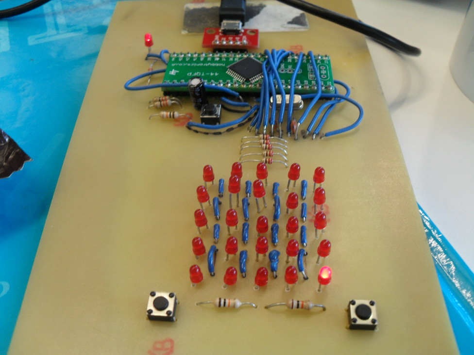
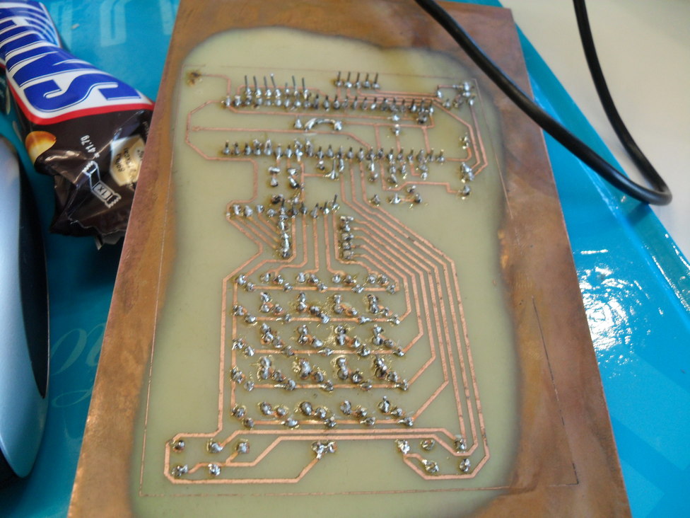
- Hand etching, hand drilling, hand soldering a PCB in the kitchen.
- Getting a first board created by DF Robot, flow soldering in the kitchen
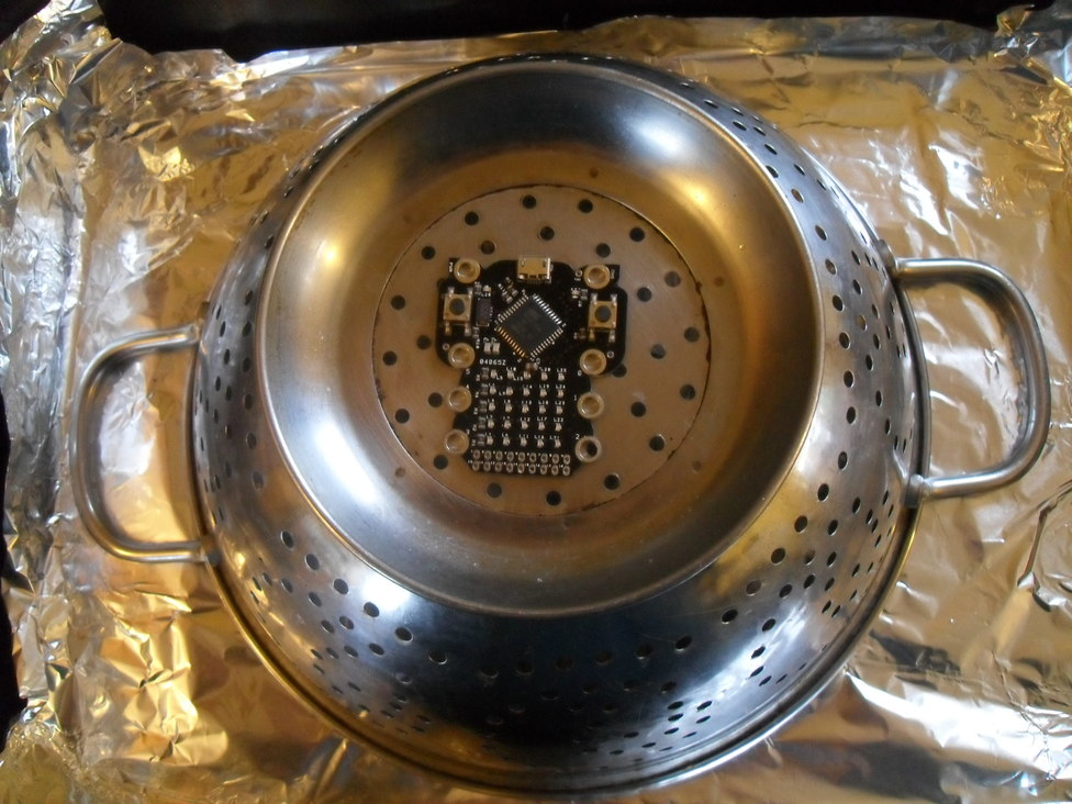
- Getting the “final” hand made board created by DF Robot, hand assembled and flow soldered in the kitchen. (on top of the cooker using a heat gun)
The reason for mentioning this is when it came to this final one, I’d realised that taking photographs during that process would be useful for myself to check alignment of components before flow soldering, and might be interesting for others later… (Zoom on a camera being far better than a human’s eyes after all)
- KRYTEN: Now then, uh, my optical system doesn’t appear to have a zoom function.
Early Pictures
Anyway, the first three devices looked like this:
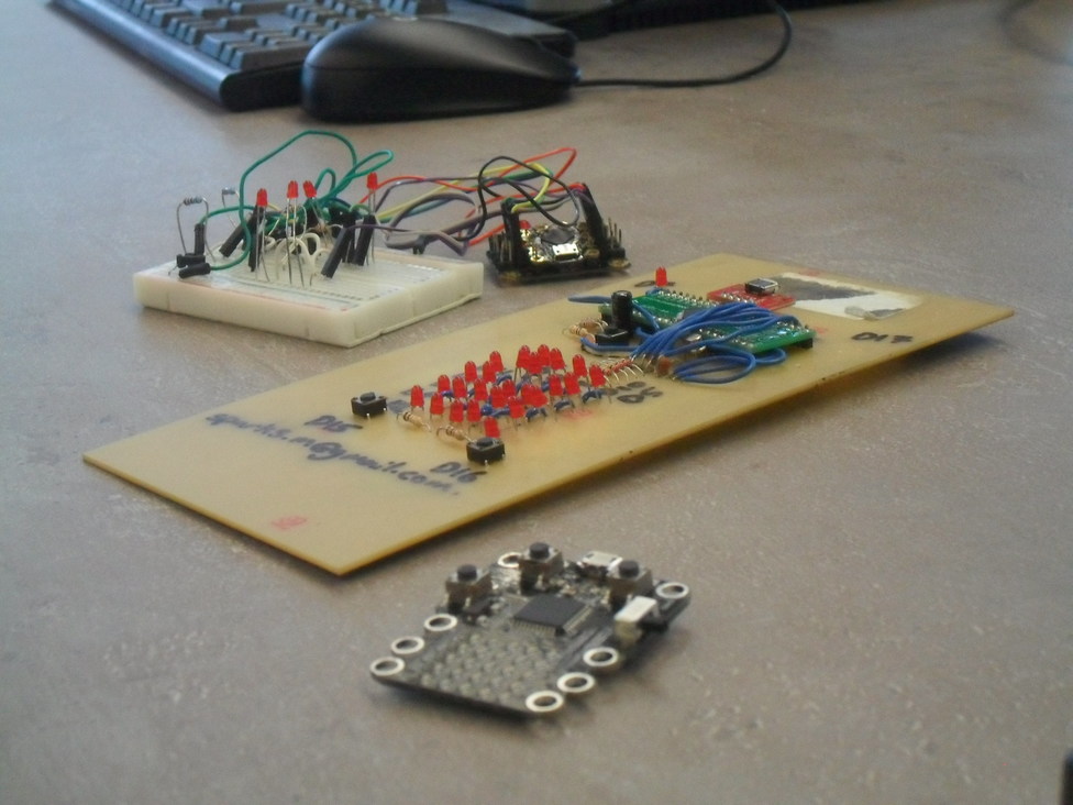
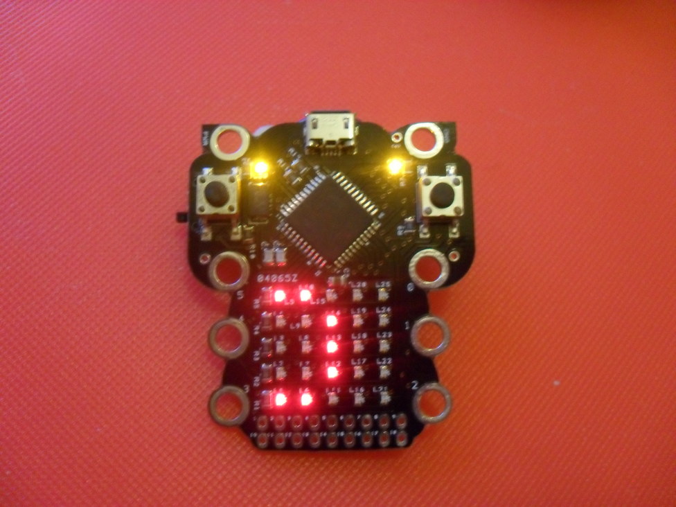
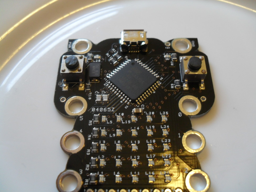
The fourth - the last manually assembled device - looked like this: (I was going for kitten and it looked vaguely owl shaped :-)
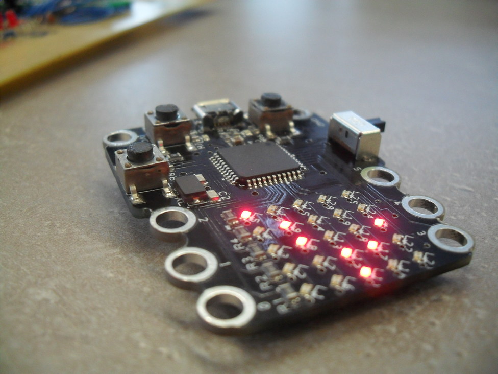
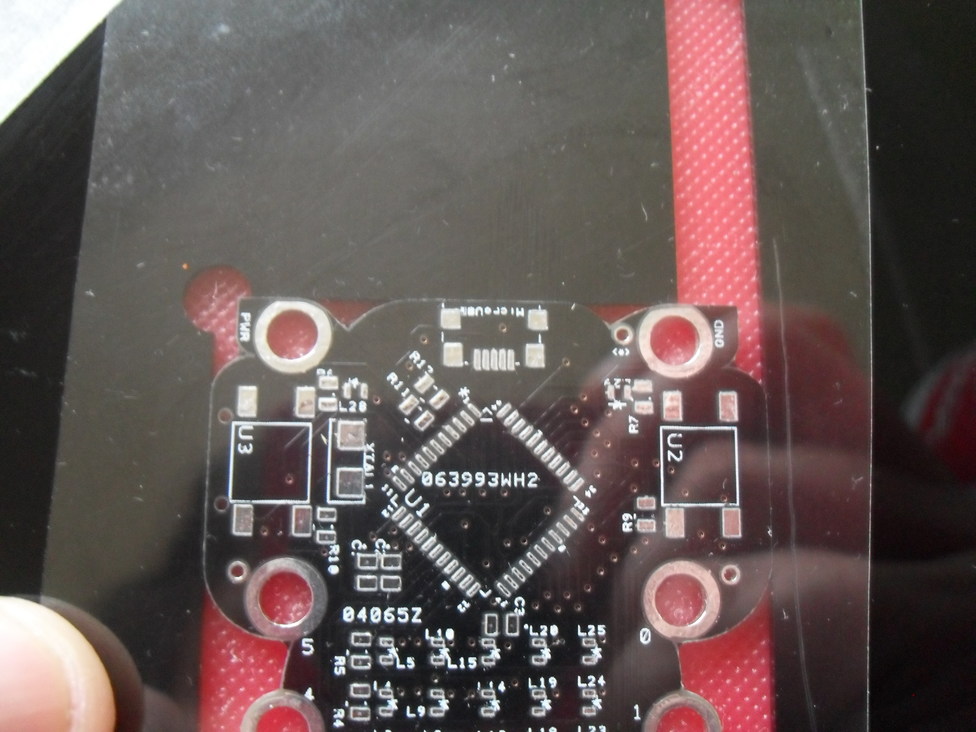
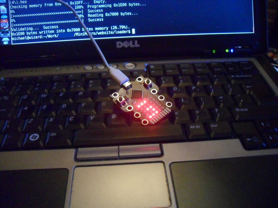
And of course the “final” device looked like this below. The changes here are to enable many boards to be printed together, pick and place machines to deposit components, and allow boards to be easily split and to minimise wastage. Still the same design otherwise though :)
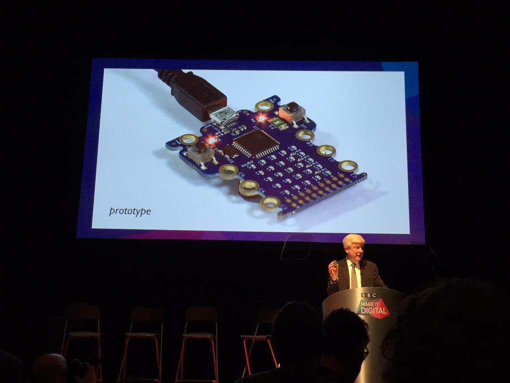
… of which 1000 were machine manufactured - 500 went into schools in the original Pilot schools-trial in Jan 2015, 500 were for potential partners. (We didn’t know if we’d even get any partners then)
Gallery
A (simple) gallery of various different photos I took during that early stage is here:
Some highlights are below.
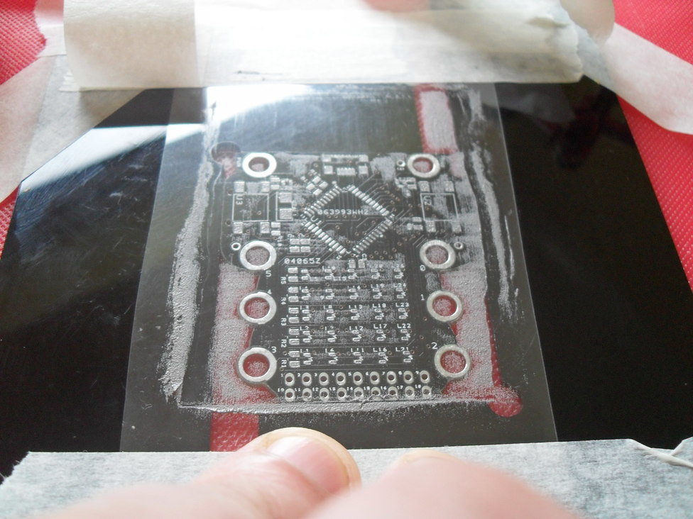
Hand etched device front, back and first surfacemount/hand assembled device
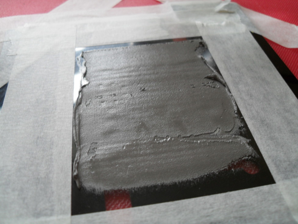
Using a stencil to apply solder paste:
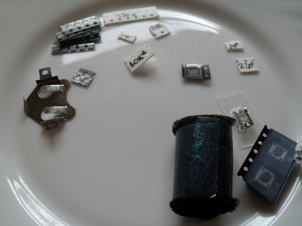
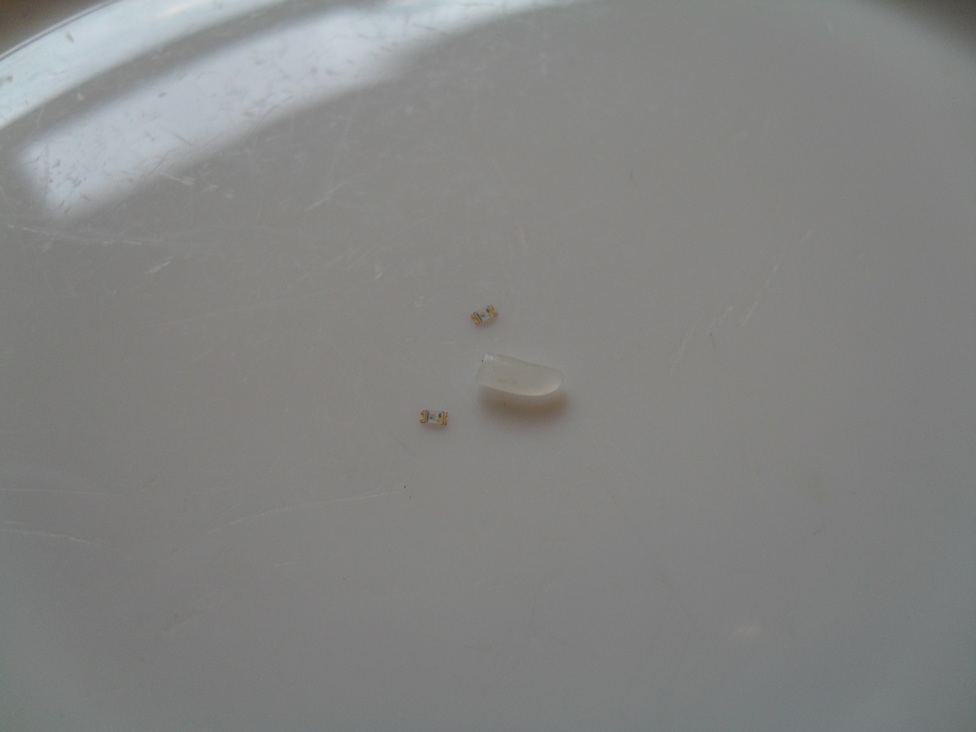
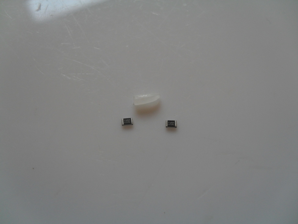
The components needed to build a prototype device by hand, grain of rice for scale:
Using a camera to check alignment of components before then putting on cooker to point a heat gun, and then checking things afterwards. Note the slight wobble of components before that surface tension fixes when the solder melts:
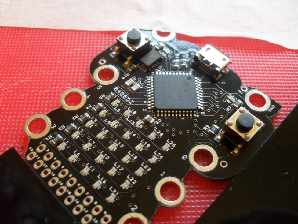
You can tell the before/after due to the slightly melted buttons!
Some running pictures & back:
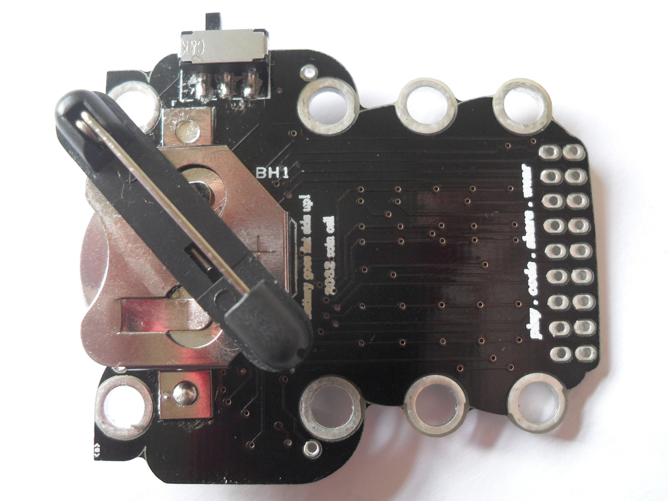
Two things of note from the back:
Personal inspiration
<*>- Babylon 5 has a great quote in it’s Pilot episode of the power of one mind to effect change. It’s a show about consequences, responsibility - but also one of effecting change in the world against difficult odds. The<*>is an old symbol from old online B5 fans from the 90s (usenet) and it just seemed appropriate to me then. This survived through to the machine manufactured version for the Pilot :-)The other was a little motto - which again made it through to the machine manufactured version - of “play . code . share . wear” - the 4 main things we wanted people to get from the device.
Hand etching?
Yes you can hand etch a printed PCB in the kitchen. Unfortunately I don’t have photos of this process. If you have a laser printer, a single layer copper backed PCB board, and ferric chloride - you can easily etch at home. What you do is:
- Create a mirror image of your circuit.
- Print that using a laser printer
- Clean the copper side of the PCB using alcohol or acetone. (A major ingredient in many nail polish removers, as was a major plot point in the Moonbase/Cyberman Doctor Who story)
- Then place the toner side of your print out against the copper
- Iron the laser printed image onto the copper. This transfers the toner from the paper to the copper. This is much like when you used to iron pictures onto t-shirts.
- Allow it to cool
- Gentle peel off the paper - leaving the toner on the copper
- The toner then protects the copper
- Wearing gloves gently rub ferric chloride onto the copper using a sponge wearing gloves - this etches the copper away, leaving the copper. (Hence the “cloud edging” shape around the copper tracks) (this youtube video gives an idea of what this looks like)
- Rinse the board well.
- Clean off the laser toner. (Again the acetone/nail polish remover.)
- Drill the holes in the board - being careful to not lift the tracks. Amusingly the drill bits you use for this are called “microbits”
Lastly, you then hand solder your components. In my case, badly - but it got me a dev-kit :)
Don’t pour ferric chloride down the sink Aside from environmental concerns, if your plumbing is made of copper, you’ll risk destroying it.
Summing up
For various reasons they later decided to call this Pilot version the prototype, but when this was being made, we had no idea if partners would come on board and if they did whether anyone would be willing to say “I can do better”. So at the time, that Pilot version was all there was, so the hand made devices were always to me the prototypes, and the final blue (Tardis like) one was the production device.
So that’s it really, just an excuse to share some old photos, in the hope that they’re interesting. It shows that if you want to build one of these things yourself, you can actually do it.
I never actually claimed back any costs I incurred in these early devices, which tells you it was actually a cheap process. If you didn’t have the time pressures I had this becomes even more achievable.
So, if you’ve ever thought of doing a kickstarter, this should give you some idea how practical this can be to iterate hardware - even PCB based hardware.
Updated: 2026/03/02 23:17:42